We currently offer the following types of membrane chips and provide detailed instructions on related experimental aspects (how to use the chips, how to store them, how to clean them etc., as documented by our scientists who are using these products in their own Research & Development Work).
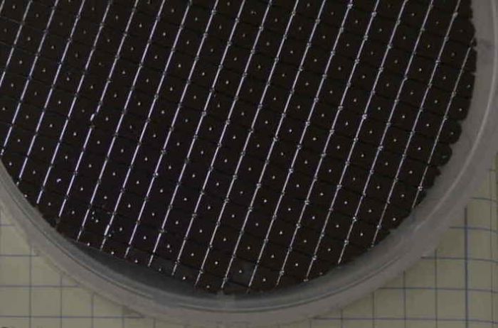
The products include: membranes only, membranes with nanopores, SiN pores, 2D material pores, single and multiple pore chips (nanopore arrays), chips with additional features such as metal patterns for a range of applications (examples are metal electrodes). Chips can be coated for specific applications and we offer those services as well. Currently, we have in stock chip shapes and dimensions from 3mm, 5×4 mm and 5x5mm in stock. See our Blog for examples of studies facilitated by our products.
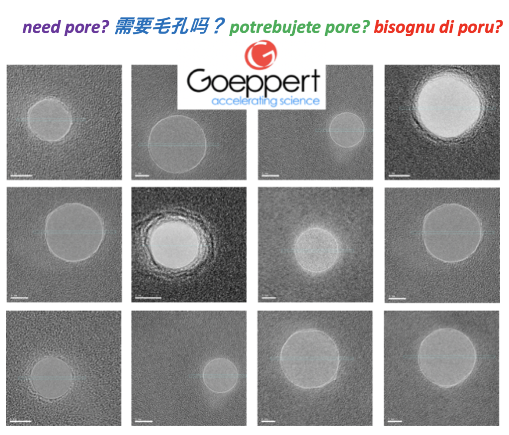
Nanopore chips come with TEM-images with measured sizes. Additional characterizations such as structural & elemental analyses are performed upon request. Our team is unique in that we specialize both in measurements and fabrication and can offer help with measurements, as well as perform measurements on your samples, as needed.
We sell standard and custom-made chips with nanopore diameters from 1 nm to 100’s of nm’s in membrane thicknesses from atomically-thin (2D materials) to thicker up to about 100 nm-thick-channels.
We ship them in packs of 5 and 10. Please contact us for a quote with nanopore diameters, thicknesses and any other specifications. We offer steep discounts for larger orders (more than 50 chips) and the lowest prices currently on the market.
Each chip comes with full characterization and specifications. Pore diameter tolerance is +/- 0.1 nm for small pores and 1-2 nm for larger pores. Unlike TEM-based window platforms that produce higher noise, our chips are optimized for nanopore electrical measurements. Email us with desired specifications at: info@gppert.com, or info@goeppert.space.
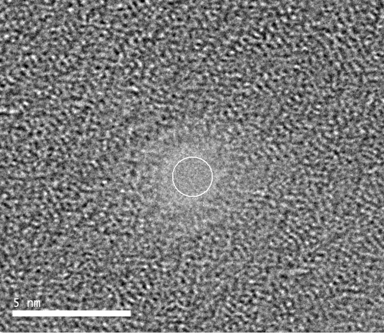
Example of a ~ 1.7 nm diameter SiN pore in 20-nm-thick SiN supporting membranes.
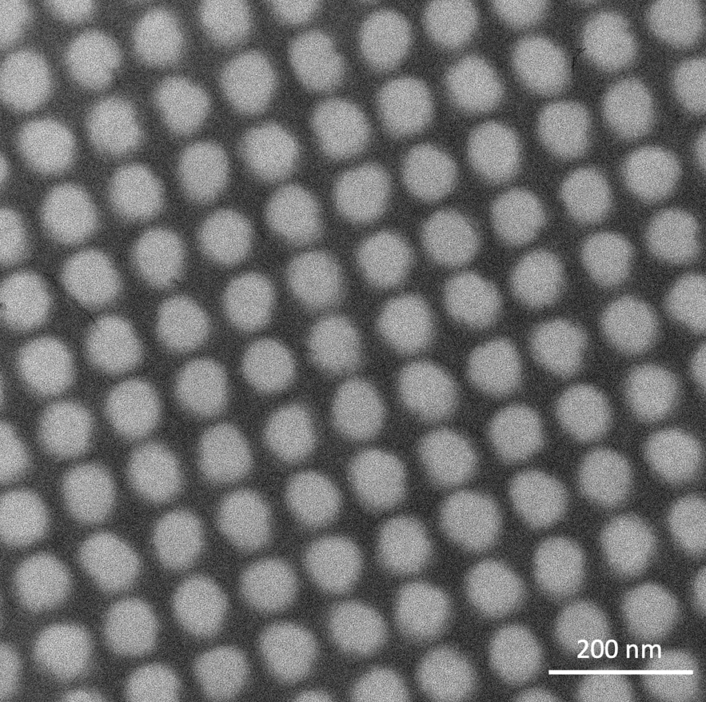
Example of SiN nanopore array chips: